

What Makes A Register Different Than A Lot Of The Other Hardware Such As A (De)mux Or (En/de)coder?
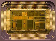
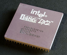 An Intel 80486DX2 CPU, as seen from above
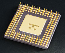 Bottom side of an Intel 80486DX2
A central processing unit (CPU) is the electronic circuitry within a computer that carries out the instructions of a figurer programme past performing the bones arithmetic, logical, control and input/output (I/O) operations specified past the instructions. The term has been used in the calculator industry at least since the early 1960s. Traditionally, the term "CPU" refers to a processor, more specifically to its processing unit and control unit (CU), distinguishing these core elements of a computer from external components such as main memory and I/O circuitry.
The grade, blueprint and implementation of CPUs have changed over the class of their history, but their fundamental operation remains nearly unchanged. Principal components of a CPU include the arithmetic logic unit (ALU) that performs arithmetic and logic operations, processor registers that supply operands to the ALU and store the results of ALU operations, and a control unit that fetches instructions from retentiveness and "executes" them by directing the coordinated operations of the ALU, registers and other components.
About mod CPUs are microprocessors, meaning they are contained on a single integrated excursion (IC) fleck. An IC that contains a CPU may besides comprise memory, peripheral interfaces, and other components of a estimator; such integrated devices are variously calledmicrocontrollers or systems on a scrap (SoC). Some computers employ a multi-cadre processor, which is a unmarried bit containing two or more than CPUs called "cores"; in that context, single chips are sometimes referred to equally "sockets". Array processors or vector processors have multiple processors that operate in parallel, with no unit of measurement considered central.
History
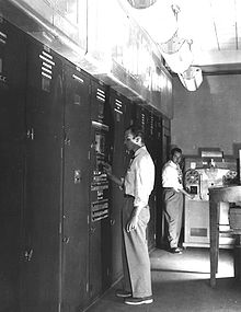 EDVAC, 1 of the first stored-program computers
Computers such as the ENIAC had to exist physically rewired to perform different tasks, which caused these machines to exist called "fixed-program computers".Since the term "CPU" is mostly divers every bit a device for software (reckoner program) execution, the earliest devices that could rightly be called CPUs came with the advent of the stored-program reckoner.
The idea of a stored-program calculator was already nowadays in the design of J. Presper Eckert and John William Mauchly'south ENIAC, but was initially omitted so that it could exist finished sooner.On June 30, 1945, before ENIAC was made, mathematician John von Neumann distributed the paper entitled Kickoff Draft of a Written report on the EDVAC. Information technology was the outline of a stored-program computer that would eventually be completed in Baronial 1949.EDVAC was designed to perform a certain number of instructions (or operations) of diverse types. Significantly, the programs written for EDVAC were to exist stored in high-speed estimator retentivity rather than specified by the physical wiring of the figurer. This overcame a severe limitation of ENIAC, which was the considerable time and endeavor required to reconfigure the calculator to perform a new chore. With von Neumann'due south design, the program that EDVAC ran could exist inverse simply past changing the contents of the memory. EDVAC, all the same, was not the commencement stored-programme computer; the Manchester Pocket-sized-Scale Experimental Machine, a small prototype stored-plan figurer, ran its first program on 21 June 1948and the Manchester Mark i ran its offset program during the night of sixteen–17 June 1949.
Early CPUs were custom designs used as part of a larger and sometimes distinctive computer. Still, this method of designing custom CPUs for a particular application has largely given way to the development of multi-purpose processors produced in large quantities. This standardization began in the era of discrete transistor mainframes and minicomputers and has rapidly accelerated with the popularization of the integrated circuit (IC). The IC has allowed increasingly circuitous CPUs to exist designed and manufactured to tolerances on the order of nanometers.Both the miniaturization and standardization of CPUs take increased the presence of digital devices in modern life far beyond the express application of dedicated computing machines. Modern microprocessors appear in electronic devices ranging from automobiles to cellphones, and sometimes even in children's toys.
While von Neumann is most often credited with the design of the stored-program computer because of his blueprint of EDVAC, and the design became known as the von Neumann compages, others earlier him, such as Konrad Zuse, had suggested and implemented like ideas. The so-called Harvard compages of the Harvard Mark I, which was completed before EDVAC, likewise utilized a stored-program design using punched paper tape rather than electronic memory. The key difference between the von Neumann and Harvard architectures is that the latter separates the storage and handling of CPU instructions and data, while the former uses the same retentiveness space for both. Most modern CPUs are primarily von Neumann in design, just CPUs with the Harvard compages are seen every bit well, specially in embedded applications; for instance, the Atmel AVR microcontrollers are Harvard architecture processors.
Relays and vacuum tubes (thermionic tubes) were commonly used every bit switching elements; a useful computer requires thousands or tens of thousands of switching devices. The overall speed of a organisation is dependent on the speed of the switches. Tube computers like EDVAC tended to boilerplate eight hours betwixt failures, whereas relay computers like the (slower, simply earlier) Harvard Marking I failed very rarely. In the stop, tube-based CPUs became dominant because the meaning speed advantages afforded mostly outweighed the reliability problems. Most of these early on synchronous CPUs ran at low clock rates compared to modern microelectronic designs (see below for a discussion of clock rate). Clock signal frequencies ranging from 100 kHz to 4 MHz were very common at this time, limited largely by the speed of the switching devices they were built with.
Transistor CPUs
The design complexity of CPUs increased equally diverse technologies facilitated building smaller and more reliable electronic devices. The start such improvement came with the advent of the transistor. Transistorized CPUs during the 1950s and 1960s no longer had to be built out of bulky, unreliable, and fragile switching elements like vacuum tubes and relays. With this comeback more complex and reliable CPUs were built onto one or several printed circuit boards containing discrete (individual) components.
In 1964, IBM introduced its Arrangement/360 computer compages that was used in a series of computers capable of running the same programs with different speed and operation. This was meaning at a time when virtually electronic computers were incompatible with i another, even those made by the aforementioned manufacturer. To facilitate this comeback, IBM utilized the concept of a microprogram (frequently called "microcode"), which still sees widespread usage in modern CPUs.The Arrangement/360 compages was so popular that information technology dominated the mainframe computer market for decades and left a legacy that is notwithstanding continued by like modern computers like the IBM zSeries. In 1965, Digital Equipment Corporation (DEC) introduced some other influential computer aimed at the scientific and research markets, the PDP-viii.
Transistor-based computers had several distinct advantages over their predecessors. Aside from facilitating increased reliability and lower power consumption, transistors also immune CPUs to operate at much higher speeds because of the short switching fourth dimension of a transistor in comparison to a tube or relay. Thanks to both the increased reliability as well as the dramatically increased speed of the switching elements (which were well-nigh exclusively transistors by this time), CPU clock rates in the tens of megahertz were obtained during this period. Additionally while discrete transistor and IC CPUs were in heavy usage, new high-performance designs like SIMD (Single Instruction Multiple Data) vector processors began to appear. These early experimental designs later gave ascension to the era of specialized supercomputers like those made past Cray Inc.
Small-scale-scale integration CPUs
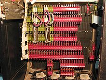 CPU, core retention, and external bus interface of a Dec PDP-8/I. Made of medium-scale integrated circuits.
During this menstruation, a method of manufacturing many interconnected transistors in a compact infinite was developed. The integrated circuit (IC) allowed a large number of transistors to exist manufactured on a single semiconductor-based die, or "scrap". At first only very basic non-specialized digital circuits such as NOR gates were miniaturized into ICs. CPUs based upon these "edifice block" ICs are mostly referred to as "small-scale integration" (SSI) devices. SSI ICs, such as the ones used in the Apollo guidance figurer, usually contained upwards to a few score transistors. To build an unabridged CPU out of SSI ICs required thousands of individual fries, merely still consumed much less space and power than earlier discrete transistor designs.
IBM's Arrangement/370 follow-on to the System/360 used SSI ICs rather than Solid Logic Technology discrete-transistor modules. Dec's PDP-8/I and KI10 PDP-x also switched from the individual transistors used past the PDP-8 and PDP-x to SSI ICs, and their extremely popular PDP-11line was originally congenital with SSI ICs but was eventually implemented with LSI components one time these became practical.
Large-scale integration CPUs
Lee Boysel published influential articles, including a 1967 "manifesto", which described how to build the equivalent of a 32-flake mainframe reckoner from a relatively small number of large-scale integration circuits (LSI). At the time, the only way to build LSI chips, which are chips with a hundred or more gates, was to build them using a MOS process (i.e.,PMOS logic, NMOS logic, or CMOS logic). However, some companies continued to build processors out of bipolar chips because bipolar junction transistors were and so much faster than MOS chips; for case, Datapoint built processors out of TTL fries until the early 1980s.
People building high-speed computers wanted them to be fast, so in the 1970s they built the CPUs from minor integration (SSI) and medium-scale integration (MSI) 7400 seriesTTL gates. At the time, MOS ICs were so irksome that they were considered useful merely in a few niche applications that required low power. As the microelectronic technology advanced, an increasing number of transistors were placed on ICs, decreasing the quantity of private ICs needed for a complete CPU. MSI and LSI ICs increased transistor counts to hundreds, and then thousands. By 1968, the number of ICs required to build a complete CPU had been reduced to 24 ICs of eight different types, with each IC containing roughly 1000 MOSFETs.In stark dissimilarity with its SSI and MSI predecessors, the first LSI implementation of the PDP-11 contained a CPU composed of simply four LSI integrated circuits.
Microprocessors
 Die of an Intel 80486DX2microprocessor (actual size: 12×6.75 mm) in its packaging
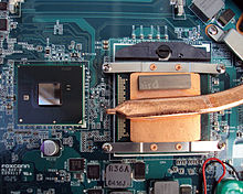 Intel Core i5 CPU on a Vaio Eastward series laptop motherboard (on the right, beneath the heat piping)
In the 1970s the key inventions by Federico Faggin (Silicon Gate MOS ICs with cocky-aligned gates along with his new random logic blueprint methodology) changed the blueprint and implementation of CPUs forever. Since the introduction of the showtime commercially available microprocessor (the Intel 4004) in 1970, and the first widely used microprocessor (the Intel 8080) in 1974, this class of CPUs has most completely overtaken all other central processing unit implementation methods. Mainframe and minicomputer manufacturers of the time launched proprietary IC evolution programs to upgrade their older reckoner architectures, and eventually produced instruction set uniform microprocessors that were backward-compatible with their older hardware and software. Combined with the advent and eventual success of the ubiquitous personal computer, the term CPU is at present applied near exclusively to microprocessors. Several CPUs (denotedcores) tin can exist combined in a unmarried processing chip.
Previous generations of CPUs were implemented as detached components and numerous small integrated circuits (ICs) on one or more circuit boards.Microprocessors, on the other hand, are CPUs manufactured on a very pocket-size number of ICs; usually just one. The overall smaller CPU size, as a outcome of existence implemented on a single dice, ways faster switching time considering of physical factors like decreased gate parasitic capacitance.This has immune synchronous microprocessors to have clock rates ranging from tens of megahertz to several gigahertz. Additionally, every bit the ability to construct exceedingly small transistors on an IC has increased, the complication and number of transistors in a single CPU has increased many fold. This widely observed trend is described by Moore's law, which has proven to exist a fairly accurate predictor of the growth of CPU (and other IC) complexity.
While the complication, size, construction, and general form of CPUs take inverse enormously since 1950, it is notable that the basic pattern and office has not changed much at all. About all mutual CPUs today tin be very accurately described as von Neumann stored-program machines. Every bit the same Moore's law continues to hold true,concerns have arisen about the limits of integrated excursion transistor technology. Extreme miniaturization of electronic gates is causing the effects of phenomena like electromigration and subthreshold leakage to get much more significant. These newer concerns are amongst the many factors causing researchers to investigate new methods of computing such as the quantum computer, as well as to aggrandize the usage of parallelism and other methods that extend the usefulness of the classical von Neumann model.
Operation
The fundamental operation of most CPUs, regardless of the physical form they take, is to execute a sequence of stored instructions that is called a program. The instructions to exist executed are kept in some kind of reckoner memory. Nearly all CPUs follow the fetch, decode and execute steps in their performance, which are collectively known equally the instruction cycle.
Afterwards the execution of an education, the entire process repeats, with the next instruction cycle normally fetching the adjacent-in-sequence instruction because of the incremented value in the program counter. If a leap instruction was executed, the program counter volition be modified to contain the accost of the didactics that was jumped to and program execution continues usually. In more circuitous CPUs, multiple instructions can be fetched, decoded, and executed simultaneously. This section describes what is by and large referred to as the "archetype RISC pipeline", which is quite common among the elementary CPUs used in many electronic devices (often called microcontroller). It largely ignores the important role of CPU cache, and therefore the access stage of the pipeline.
Some instructions dispense the plan counter rather than producing result data directly; such instructions are generally called "jumps" and facilitate program behavior like loops, conditional plan execution (through the use of a provisional jump), and existence of functions.In some processors, some other instructions change the state of bits in a "flags" register. These flags tin be used to influence how a program behaves, since they ofttimes indicate the consequence of various operations. For example, in such processors a "compare" instruction evaluates two values and sets or clears bits in the flags register to indicate which one is greater or whether they are equal; one of these flags could then be used by a later jump instruction to determine plan flow.
Fetch
The starting time footstep, fetch, involves retrieving an instruction (which is represented past a number or sequence of numbers) from program retentivity. The instruction's location (address) in program memory is adamant by a program counter (PC), which stores a number that identifies the address of the next didactics to be fetched. Subsequently an instruction is fetched, the PC is incremented past the length of the instruction then that it volition comprise the address of the next instruction in the sequence.Often, the instruction to be fetched must be retrieved from relatively irksome memory, causing the CPU to stall while waiting for the instruction to be returned. This issue is largely addressed in modern processors past caches and pipeline architectures (see below).
Decode
The instruction that the CPU fetches from retentiveness determines what the CPU will do. In the decode stride, performed by the circuitry known as the educational activity decoder, the instruction is converted into signals that command other parts of the CPU.
The way in which the pedagogy is interpreted is divers by the CPU'due south instruction set architecture (ISA). Often, one group of bits (that is, a "field") within the instruction, called the opcode, indicates which functioning is to exist performed, while the remaining fields commonly provide supplemental data required for the functioning, such every bit the operands. Those operands may exist specified equally a constant value (called an immediate value), or equally the location of a value that may be a processor register or a retention address, equally determined by some addressing mode.
In some CPU designs the instruction decoder is implemented as a hardwired, unchangeable circuit. In others, a microprogram is used to translate instructions into sets of CPU configuration signals that are applied sequentially over multiple clock pulses. In some cases the retentiveness that stores the microprogram is rewritable, making it possible to change the way in which the CPU decodes instructions.
Execute
Subsequently the fetch and decode steps, the execute step is performed. Depending on the CPU architecture, this may consist of a single action or a sequence of deportment. During each action, various parts of the CPU are electrically connected so they can perform all or part of the desired performance and then the action is completed, typically in response to a clock pulse. Very often the results are written to an internal CPU register for quick access by subsequent instructions. In other cases results may be written to slower, but less expensive and higher chapters master retentiveness.
For example, if an addition instruction is to be executed, the arithmetic logic unit (ALU) inputs are connected to a pair of operand sources (numbers to exist summed), the ALU is configured to perform an addition functioning then that the sum of its operand inputs will appear at its output, and the ALU output is connected to storage (e.thou., a register or retention) that will receive the sum. When the clock pulse occurs, the sum will be transferred to storage and, if the resulting sum is as well large (i.east., it is larger than the ALU'southward output word size), an arithmetic overflow flag will be ready.
Structure and implementation
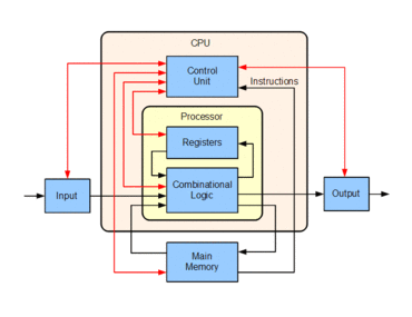 Block diagram of a bones uniprocessor-CPU reckoner. Black lines point information flow, whereas red lines indicate control menstruation; arrows point menstruation directions.
Hardwired into a CPU's circuitry is a ready of basic operations it can perform, called an didactics prepare. Such operations may involve, for case, adding or subtracting 2 numbers, comparison 2 numbers, or jumping to a different function of a programme. Each bones operation is represented past a particular combination of bits, known equally the machine language opcode; while executing instructions in a motorcar language programme, the CPU decides which performance to perform by "decoding" the opcode. A complete motorcar language instruction consists of an opcode and, in many cases, additional $.25 that specify arguments for the performance (for case, the numbers to be summed in the instance of an add-on operation). Going upwardly the complexity scale, a motorcar linguistic communication program is a collection of car language instructions that the CPU executes.
The actual mathematical operation for each instruction is performed past a combinational logic circuit within the CPU's processor known as the arithmetic logic unit or ALU. In general, a CPU executes an instruction by fetching information technology from memory, using its ALU to perform an functioning, then storing the result to memory. Abreast the instructions for integer mathematics and logic operations, various other machine instructions exist, such every bit those for loading data from memory and storing information technology back, branching operations, and mathematical operations on floating-point numbers performed by the CPU's floating-point unit (FPU).
Control unit
The control unit of the CPU contains circuitry that uses electrical signals to direct the entire computer system to carry out stored program instructions. The control unit of measurement does not execute program instructions; rather, it directs other parts of the system to exercise so. The control unit communicates with both the ALU and retention.
Arithmetic logic unit
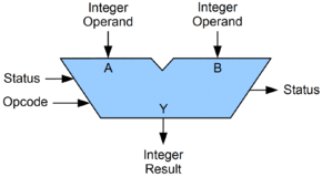 Symbolic representation of an ALU and its input and output signals
The arithmetic logic unit (ALU) is a digital circuit within the processor that performs integer arithmetic and bitwise logic operations. The inputs to the ALU are the data words to be operated on (called operands), status data from previous operations, and a code from the control unit indicating which performance to perform. Depending on the pedagogy being executed, the operands may come from internal CPU registers or external retention, or they may be constants generated by the ALU itself.
When all input signals have settled and propagated through the ALU circuitry, the event of the performed operation appears at the ALU's outputs. The outcome consists of both a information give-and-take, which may be stored in a register or memory, and status information that is typically stored in a special, internal CPU register reserved for this purpose.
Integer range
Every CPU represents numerical values in a specific way. For example, some early digital computers represented numbers equally familiar decimal (base 10) numeral system values, and others have employed more unusual representations such every bit ternary (base iii). Nigh all modern CPUs represent numbers in binary form, with each digit being represented past some ii-valued physical quantity such as a "loftier" or "low" voltage.
 A vi-bit word containing the binary encoded representation of decimal value 40. Nigh modern CPUs apply word sizes that are a power of two, for example eight, xvi, 32 or 64 bits.
Related to numeric representation is the size and precision of integer numbers that a CPU can correspond. In the case of a binary CPU, this is measured by the number of bits (significant digits of a binary encoded integer) that the CPU tin can process in one operation, which is commonly called "word size", "bit width", "data path width", "integer precision", or "integer size". A CPU's integer size determines the range of integer values it can direct operate on. For example, an viii-scrap CPU can directly manipulate integers represented by viii bits, which have a range of 256 (28) discrete integer values.
Integer range can besides affect the number of memory locations the CPU can directly accost (an address is an integer value representing a specific memory location). For instance, if a binary CPU uses 32 bits to represent a memory address then it can directly accost two32 retention locations. To circumvent this limitation and for various other reasons, some CPUs employ mechanisms (such as depository financial institution switching) that allow additional retentiveness to be addressed.
CPUs with larger word sizes require more circuitry and consequently are physically larger, cost more than, and consume more power (and therefore generate more heat). Every bit a event, smaller 4- or 8-fleck microcontrollers are commonly used in modern applications fifty-fifty though CPUs with much larger word sizes (such as xvi, 32, 64, fifty-fifty 128-chip) are available. When higher performance is required, however, the benefits of a larger discussion size (larger data ranges and accost spaces) may outweigh the disadvantages.
To gain some of the advantages afforded past both lower and higher bit lengths, many CPUs are designed with dissimilar bit widths for dissimilar portions of the device. For case, the IBM System/370 used a CPU that was primarily 32 bit, but it used 128-flake precision inside its floating point units to facilitate greater accuracy and range in floating indicate numbers.Many later CPU designs use like mixed bit width, especially when the processor is meant for general-purpose usage where a reasonable balance of integer and floating bespeak capability is required.
Clock rate
Most CPUs are synchronous circuits, which ways they employ a clock point to pace their sequential operations. The clock signal is produced past an external oscillator circuit that generates a consistent number of pulses each second in the form of a periodic square moving ridge. The frequency of the clock pulses determines the rate at which a CPU executes instructions and, consequently, the faster the clock, the more instructions the CPU will execute each second.
To ensure proper operation of the CPU, the clock menstruum is longer than the maximum time needed for all signals to propagate (movement) through the CPU. In setting the clock period to a value well above the worst-case propagation filibuster, information technology is possible to design the entire CPU and the fashion it moves data effectually the "edges" of the ascent and falling clock point. This has the advantage of simplifying the CPU significantly, both from a blueprint perspective and a component-count perspective. Notwithstanding, information technology as well carries the disadvantage that the entire CPU must wait on its slowest elements, fifty-fifty though some portions of it are much faster. This limitation has largely been compensated for by various methods of increasing CPU parallelism (run into below).
However, architectural improvements alone do not solve all of the drawbacks of globally synchronous CPUs. For example, a clock indicate is subject to the delays of any other electric point. Higher clock rates in increasingly complex CPUs get in more difficult to keep the clock signal in phase (synchronized) throughout the entire unit. This has led many modern CPUs to crave multiple identical clock signals to be provided to avoid delaying a single bespeak significantly enough to cause the CPU to malfunction. Another major effect, as clock rates increase dramatically, is the corporeality of estrus that is prodigal by the CPU. The constantly changing clock causes many components to switch regardless of whether they are being used at that time. In general, a component that is switching uses more energy than an chemical element in a static state. Therefore, as clock rate increases, so does free energy consumption, causing the CPU to require more rut dissipation in the course of CPU cooling solutions.
One method of dealing with the switching of unneeded components is called clock gating, which involves turning off the clock point to unneeded components (effectively disabling them). Notwithstanding, this is oft regarded as hard to implement and therefore does not see common usage outside of very low-ability designs. One notable recent CPU design that uses extensive clock gating is the IBM PowerPC-based Xenon used in the Xbox 360; that way, power requirements of the Xbox 360 are greatly reduced. Some other method of addressing some of the problems with a global clock indicate is the removal of the clock signal altogether. While removing the global clock point makes the design procedure considerably more than circuitous in many ways, asynchronous (or clockless) designs deport marked advantages in power consumption and rut dissipation in comparison with similar synchronous designs. While somewhat uncommon, entire asynchronous CPUs take been built without utilizing a global clock signal. 2 notable examples of this are the ARM compliant AMULETand the MIPS R3000 compatible MiniMIPS.
Rather than totally removing the clock signal, some CPU designs permit sure portions of the device to exist asynchronous, such as using asynchronous ALUs in conjunction with superscalar pipelining to achieve some arithmetic performance gains. While information technology is not birthday clear whether totally asynchronous designs can perform at a comparable or better level than their synchronous counterparts, it is evident that they do at least excel in simpler math operations. This, combined with their fantabulous power consumption and heat dissipation properties, makes them very suitable for embedded computers.
Parallelism
 Model of a subscalar CPU, in which it takes fifteen clock cycles to complete three instructions.
The description of the basic operation of a CPU offered in the previous section describes the simplest class that a CPU can accept. This type of CPU, usually referred to as subscalar, operates on and executes one teaching on 1 or two pieces of information at a time, that is less than one education per clock wheel—or more i clock bicycle per pedagogy (CPI > i).
This process gives rise to an inherent inefficiency in subscalar CPUs. Since but one didactics is executed at a time, the entire CPU must expect for that instruction to complete before proceeding to the adjacent instruction. Every bit a issue, the subscalar CPU gets "hung upward" on instructions which have more than than ane clock bike to consummate execution. Even adding a second execution unit of measurement (see below) does non improve performance much; rather than ane pathway beingness hung up, now 2 pathways are hung up and the number of unused transistors is increased. This design, wherein the CPU's execution resources can operate on merely i instruction at a fourth dimension, tin can only mayhap accomplishscalar performance (one didactics per clock cycle or CPI = i). Withal, the performance is near always subscalar (less than 1 instruction per clock cycle or CPI > one).
Attempts to reach scalar and meliorate functioning take resulted in a variety of design methodologies that cause the CPU to behave less linearly and more in parallel. When referring to parallelism in CPUs, two terms are generally used to classify these blueprint techniques:
- instruction-level parallelism (ILP), which seeks to increase the rate at which instructions are executed within a CPU (that is, to increment the utilization of on-die execution resources);
- thread-level parallelism (TLP), which purposes to increase the number of threads (effectively individual programs) that a CPU can execute simultaneously.
Each methodology differs both in the ways in which they are implemented, as well as the relative effectiveness they beget in increasing the CPU's operation for an awarding.
Instruction-level parallelism
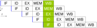 Basic five-stage pipeline. In the all-time case scenario, this pipeline tin sustain a completion rate of one didactics per cycle.
One of the simplest methods used to achieve increased parallelism is to begin the start steps of educational activity fetching and decoding earlier the prior instruction finishes executing. This is the simplest form of a technique known equally instruction pipelining, and is utilized in most all modern full general-purpose CPUs. Pipelining allows more than 1 instruction to be executed at whatever given time by breaking down the execution pathway into detached stages. This separation tin exist compared to an assembly line, in which an instruction is fabricated more consummate at each stage until information technology exits the execution pipeline and is retired.
Pipelining does, however, introduce the possibility for a situation where the result of the previous operation is needed to complete the adjacent operation; a condition often termed data dependency disharmonize. To cope with this, boosted care must be taken to check for these sorts of atmospheric condition and filibuster a portion of the education pipeline if this occurs. Naturally, accomplishing this requires additional circuitry, then pipelined processors are more complex than subscalar ones (though non very significantly so). A pipelined processor can go very almost scalar, inhibited only by pipeline stalls (an teaching spending more ane clock cycle in a phase).
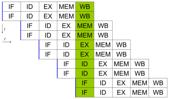 A uncomplicated superscalar pipeline. By fetching and dispatching 2 instructions at a time, a maximum of 2 instructions per cycle can be completed.
Further improvement upon the idea of didactics pipelining led to the development of a method that decreases the idle fourth dimension of CPU components even further. Designs that are said to be superscalar include a long instruction pipeline and multiple identical execution units. In a superscalar pipeline, multiple instructions are read and passed to a dispatcher, which decides whether or not the instructions tin can be executed in parallel (simultaneously). If so they are dispatched to bachelor execution units, resulting in the power for several instructions to be executed simultaneously. In full general, the more than instructions a superscalar CPU is able to dispatch simultaneously to waiting execution units, the more instructions will be completed in a given bicycle.
Most of the difficulty in the design of a superscalar CPU architecture lies in creating an effective dispatcher. The dispatcher needs to exist able to quickly and correctly make up one's mind whether instructions tin be executed in parallel, as well as dispatch them in such a manner every bit to keep as many execution units busy equally possible. This requires that the teaching pipeline is filled every bit often as possible and gives ascent to the need in superscalar architectures for significant amounts of CPU cache. It likewise makes gamble-avoiding techniques similar branch prediction, speculative execution, and out-of-lodge execution crucial to maintaining high levels of performance. By attempting to predict which co-operative (or path) a conditional education will have, the CPU tin can minimize the number of times that the entire pipeline must await until a conditional instruction is completed. Speculative execution oftentimes provides modest performance increases by executing portions of lawmaking that may not be needed later a conditional performance completes. Out-of-order execution somewhat rearranges the order in which instructions are executed to reduce delays due to data dependencies. Likewise in instance of Unmarried Instructions Multiple Data—a example when a lot of data from the same type has to be processed, modern processors can disable parts of the pipeline so that when a single pedagogy is executed many times, the CPU skips the fetch and decode phases and thus profoundly increases performance on certain occasions, especially in highly monotonous program engines such as video cosmos software and photograph processing.
In the case where a portion of the CPU is superscalar and part is not, the part which is not suffers a performance penalty due to scheduling stalls. The Intel P5 Pentium had two superscalar ALUs which could have one instruction per clock each, but its FPU could non accept one instruction per clock. Thus the P5 was integer superscalar but not floating point superscalar. Intel's successor to the P5 architecture, P6, added superscalar capabilities to its floating point features, and therefore afforded a significant increase in floating point pedagogy performance.
Both simple pipelining and superscalar design increase a CPU's ILP past assuasive a unmarried processor to complete execution of instructions at rates surpassing one instruction per cycle (IPC). Most mod CPU designs are at least somewhat superscalar, and nearly all general purpose CPUs designed in the last decade are superscalar. In afterwards years some of the accent in designing high-ILP computers has been moved out of the CPU'southward hardware and into its software interface, or ISA. The strategy of the very long instruction word (VLIW) causes some ILP to become unsaid directly by the software, reducing the amount of piece of work the CPU must perform to boost ILP and thereby reducing the design's complication.
Thread-level parallelism
Some other strategy of achieving performance is to execute multiple programs or threads in parallel. This area of research is known as parallel computing. In Flynn'southward taxonomy, this strategy is known every bit Multiple instruction stream-Multiple data stream or MIMD.
One engineering used for this purpose was multiprocessing (MP). The initial season of this engineering science is known as symmetric multiprocessing (SMP), where a small number of CPUs share a coherent view of their retentivity arrangement. In this scheme, each CPU has additional hardware to maintain a constantly up-to-date view of memory. By avoiding stale views of memory, the CPUs tin can cooperate on the aforementioned plan and programs tin can migrate from one CPU to another. To increase the number of cooperating CPUs beyond a handful, schemes such equally non-uniform memory access (NUMA) and directory-based coherence protocols were introduced in the 1990s. SMP systems are limited to a small number of CPUs while NUMA systems have been built with thousands of processors. Initially, multiprocessing was built using multiple discrete CPUs and boards to implement the interconnect betwixt the processors. When the processors and their interconnect are all implemented on a unmarried silicon chip, the engineering science is known as a multi-core processor.
It was afterwards recognized that finer-grain parallelism existed with a single program. A single plan might have several threads (or functions) that could be executed separately or in parallel. Some of the earliest examples of this applied science implemented input/output processing such every bit direct retentiveness access as a dissever thread from the ciphering thread. A more than general arroyo to this engineering was introduced in the 1970s when systems were designed to run multiple computation threads in parallel. This technology is known equally multi-threading (MT). This approach is considered more cost-constructive than multiprocessing, as merely a small number of components within a CPU is replicated to support MT as opposed to the entire CPU in the case of MP. In MT, the execution units and the memory system including the caches are shared among multiple threads. The downside of MT is that the hardware support for multithreading is more than visible to software than that of MP and thus supervisor software similar operating systems have to undergo larger changes to support MT. Ane type of MT that was implemented is known as cake multithreading, where one thread is executed until it is stalled waiting for data to return from external memory. In this scheme, the CPU would then rapidly switch to another thread which is ready to run, the switch oft done in one CPU clock cycle, such as the UltraSPARC Technology. Some other type of MT is known as simultaneous multithreading, where instructions of multiple threads are executed in parallel inside one CPU clock cycle.
For several decades from the 1970s to early 2000s, the focus in designing high functioning general purpose CPUs was largely on achieving high ILP through technologies such as pipelining, caches, superscalar execution, out-of-order execution, etc. This trend culminated in large, power-hungry CPUs such as the Intel Pentium 4. By the early on 2000s, CPU designers were thwarted from achieving higher performance from ILP techniques due to the growing disparity between CPU operating frequencies and main retentiveness operating frequencies besides equally escalating CPU ability dissipation owing to more esoteric ILP techniques.
CPU designers then borrowed ideas from commercial computing markets such as transaction processing, where the amass operation of multiple programs, also known every bit throughput computing, was more of import than the performance of a unmarried thread or program.
This reversal of emphasis is evidenced by the proliferation of dual and multiple core CMP (chip-level multiprocessing) designs and notably, Intel's newer designs resembling its less superscalar P6 architecture. Tardily designs in several processor families showroom CMP, including the x86-64 Opteron and Athlon 64 X2, the SPARC UltraSPARC T1, IBM POWER4 andPOWER5, as well as several video game console CPUs like the Xbox 360'south triple-core PowerPC design, and the PS3's vii-core Jail cell microprocessor.
Data parallelism
A less mutual but increasingly important paradigm of CPUs (and indeed, computing in general) deals with data parallelism. The processors discussed earlier are all referred to every bit some type of scalar device. Every bit the name implies, vector processors deal with multiple pieces of information in the context of one pedagogy. This contrasts with scalar processors, which deal with one piece of data for every instruction. Using Flynn's taxonomy, these two schemes of dealing with data are generally referred to as SIMD (single instruction, multiple information) and SISD (single instruction, single data), respectively. The great utility in creating CPUs that bargain with vectors of data lies in optimizing tasks that tend to require the same operation (for example, a sum or a dot product) to be performed on a big set of data. Some archetype examples of these types of tasks are multimedia applications (images, video, and sound), likewise as many types of scientific and engineering tasks. Whereas a scalar CPU must complete the entire process of fetching, decoding, and executing each didactics and value in a set of data, a vector CPU tin can perform a unmarried operation on a comparatively large set up of data with 1 instruction. Of class, this is just possible when the application tends to require many steps which utilize one operation to a large set of data.
Virtually early vector CPUs, such as the Cray-1, were associated nigh exclusively with scientific research and cryptography applications. However, equally multimedia has largely shifted to digital media, the need for some class of SIMD in general-purpose CPUs has become significant. Presently afterward inclusion of floating point execution units started to become commonplace in general-purpose processors, specifications for and implementations of SIMD execution units also began to appear for general-purpose CPUs. Some of these early SIMD specifications like HP's Multimedia Acceleration eXtensions (MAX) and Intel's MMX were integer-only. This proved to be a pregnant impediment for some software developers, since many of the applications that benefit from SIMD primarily deal with floating indicate numbers. Progressively, these early on designs were refined and remade into some of the common, modernistic SIMD specifications, which are ordinarily associated with one ISA. Some notable modern examples are Intel's SSE and the PowerPC-related AltiVec (also known as VMX).
Performance
The functioning or speed of a processor depends on, among many other factors, the clock charge per unit (generally given in multiples of hertz) and the instructions per clock (IPC), which together are the factors for the instructions per second (IPS) that the CPU tin can perform. Many reported IPS values have represented "peak" execution rates on artificial instruction sequences with few branches, whereas realistic workloads consist of a mix of instructions and applications, some of which accept longer to execute than others. The functioning of the retentiveness hierarchy as well greatly affects processor performance, an issue barely considered in MIPS calculations. Because of these bug, various standardized tests, ofttimes called"benchmarks" for this purpose—such as SPECint—accept been developed to attempt to measure the existent constructive operation in usually used applications.
Processing performance of computers is increased by using multi-core processors, which substantially is plugging two or more than individual processors (called cores in this sense) into 1 integrated excursion. Ideally, a dual core processor would exist nearly twice equally powerful equally a unmarried core processor. In do, the performance gain is far smaller, only nearly fifty%, due to imperfect software algorithms and implementation. Increasing the number of cores in a processor (i.east. dual-cadre, quad-core, etc.) increases the workload that can exist handled. This ways that the processor tin now handle numerous asynchronous events, interrupts, etc. which can take a toll on the CPU when overwhelmed. These cores can be idea of as unlike floors in a processing plant, with each floor handling a dissimilar task. Sometimes, these cores will handle the aforementioned tasks as cores side by side to them if a single core is not plenty to handle the information.
Due to specific capabilities of modern CPUs, such as hyper-threading and uncore, which involve sharing of actual CPU resource while aiming at increased utilization, monitoring operation levels and hardware utilization gradually became a more complex chore.As a response, some CPUs implement additional hardware logic that monitors actual utilization of various parts of a CPU and provides various counters accessible to software; an case is Intel's Performance Counter Monitor technology.

What Makes A Register Different Than A Lot Of The Other Hardware Such As A (De)mux Or (En/de)coder?,
Source: https://courses.lumenlearning.com/zeliite115/chapter/reading-the-central-processing-unit/
Posted by: bennettfactly.blogspot.com
0 Response to "What Makes A Register Different Than A Lot Of The Other Hardware Such As A (De)mux Or (En/de)coder?"
Post a Comment